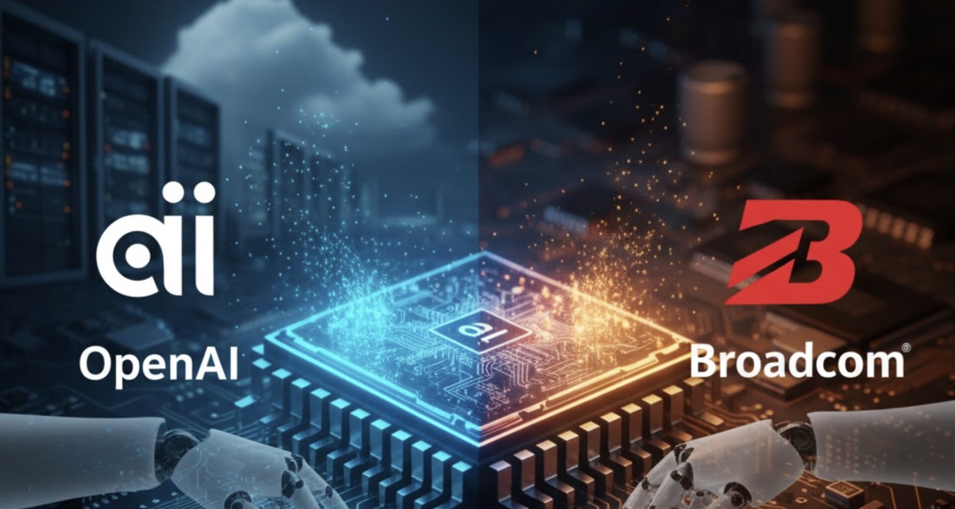

OpenAI and Broadcom announced a multi-year partnership to co-develop custom AI chips and deploy 10 gigawatts of AI computing capacity, marking one of the largest AI infrastructure build-outs to date.
Key Takeaways from the OpenAI Podcast Discussion (Video)
- Unprecedented AI Compute Demand: OpenAI’s leaders frame the scale of upcoming AI hardware needs as historically immense. Greg Brockman described the AI infrastructure build-out as possibly “the biggest joint industrial project in human history,” underscoring that meeting global AI demand will require a “gigantic amount” of computing infrastructurestartuphub.aistartuphub.ai. This reflects the broader context: advanced AI models need orders-of-magnitude more compute, pushing the limits of current data centers.
- Industry Reactions and Significance: The announcement of OpenAI’s custom chip venture sent ripples through the tech industry. Broadcom’s stock jumped ~10–12% on the newsreuters.cominvestorshub.advfn.com, as investors recognized the deal’s significance for the chipmaker. Analysts noted that while this move won’t unseat NVIDIA’s dominance overnight, it cements the trend of AI leaders developing in-house siliconreuters.comreuters.com. The partnership was even described by Broadcom’s Charlie Kawwas as “defining civilization’s next generation operating system,” highlighting its perceived importancestartuphub.ai.
- AI Compute at Extreme Scale: In the podcast, OpenAI and Broadcom emphasized the global-scale of future AI systems. Sam Altman remarked that serving the world’s AI needs will require a “gigantic” increase in computing capacitystartuphub.ai. For perspective, the planned 10 GW of custom accelerators is roughly equivalent to the power used by over 8 million U.S. homes, or about five times the output of the Hoover Damreuters.com. Such commentary puts in context the massive energy and hardware scale behind frontier AI—today’s cutting-edge models are “a drop in the bucket compared to where we need to go” on the path to more general AIstartuphub.ai.
- Full-Stack Custom Design Philosophy: A key insight from the discussion was that optimizing AI performance now demands full-stack control—from silicon to software. Brockman revealed that OpenAI and Broadcom have been co-designing a new custom AI chip for 18 months, and are also developing a “whole custom system” around itstartuphub.aistartuphub.ai. Because modern AI supercomputers are so complex, OpenAI believes that integrating custom chips with networking and software (rather than using off-the-shelf GPUs alone) is crucial for efficiency. This holistic approach, tailoring hardware to specific AI workloads, promises better performance and cost-efficiency than general-purpose solutionsstartuphub.ai.
- Toward AI’s Future (and AGI): Throughout the conversation, participants linked this hardware initiative to the broader quest for advanced AI. Hock Tan (Broadcom’s CEO) noted that engineering teams are “pushing the innovation envelope” on semiconductor tech to meet AI’s needsstartuphub.ai. OpenAI sees custom silicon as strategically important for delivering on its mission: by embedding lessons from building frontier models directly into hardware, they aim to unlock “new levels of capability and intelligence”openai.comopenai.com. In short, bespoke AI chips are viewed as a catalyst on the road to artificial general intelligence (AGI), enabling breakthroughs that current hardware might not sustainstartuphub.ai.
Summary of the OpenAI–Broadcom Announcement
The Deal: On October 13, 2025, OpenAI and Broadcom announced a strategic collaboration to develop and deploy 10 gigawatts (GW) of OpenAI-designed AI accelerators, along with Broadcom’s networking hardwareopenai.comopenai.com. This multi-year partnership runs from initial deployment in H2 2026 to completion by end of 2029, and will span multiple generations of silicon. OpenAI will design the ASIC chips and rack-scale systems, while Broadcom will handle chip development, manufacturing, and integration of its Ethernet networking solutionsopenai.comopenai.com. The goal is to build out next-generation AI supercomputers across OpenAI’s data centers and partner facilities to meet surging demand.
Technical Highlights: The custom AI accelerators are expected to be fabricated on TSMC’s cutting-edge 3 nanometer processsdxcentral.com, indicating they will leverage the latest transistor technology. Prior reports suggest these chips will use a systolic array architecture with high-bandwidth memory (HBM), similar to Google’s TPUs or NVIDIA’s GPUs in broad designsdxcentral.com. By focusing on specialized matrix-math cores (rather than general GPU logic), the chips can be optimized for training large neural networks. The entire stack will be optimized: as Broadcom’s Charlie Kawwas noted, combining custom AI ASICs with standard Ethernet networking enables a fully integrated, scalable system with favorable cost and performanceopenai.com. Notably, the clusters will rely on Ethernet (and PCIe and optical links) instead of NVIDIA’s proprietary InfiniBand interconnectopenai.comreuters.com, reflecting a design for openness and interoperability.
Scale and Timeline: The headline figure – 10 GW of AI compute – is enormous. For comparison, NVIDIA’s CEO has estimated that a 1 GW AI data center costs on the order of $50–60 billion to build (with over half that in GPU hardware)reuters.com. OpenAI’s plan, spread over 2026–2029, implies a monumental investment in data center power and infrastructure. The first racks with OpenAI’s custom accelerators are slated to come online in the second half of 2026openai.comopenai.com. Thereafter, deployments will ramp up globally, reaching the full 10 GW capacity by late 2029openai.com. This phased rollout aligns with expected availability of 3nm chips and allows time to refine the design across generations. OpenAI has already signed term sheets and long-term agreements with Broadcom to secure this development and supply pipelineopenai.comopenai.com.
Stated Goals: OpenAI’s leadership cast the partnership as critical for their mission. Sam Altman (CEO) said that developing custom accelerators will help “unlock AI’s potential” by building the infrastructure needed for more powerful modelsopenai.com. By designing its own chips, OpenAI can bake in model-specific optimizations – essentially hardware that embodies lessons from GPT-4, GPT-5, and other frontier modelsopenai.comopenai.com. Greg Brockman (President) echoed that integrating what they’ve learned directly into silicon could yield new levels of intelligence and efficiencyopenai.com. For Broadcom, the deal reinforces the importance of Ethernet-centric designs and showcases its role in AI beyond just supplying network chipsopenai.com. Broadcom’s CEO Hock Tan called the collaboration a “pivotal moment” in the pursuit of AGI, noting OpenAI’s leadership since the “ChatGPT moment” and expressing excitement to “co-develop and deploy 10 GW of next-generation accelerators” for the future of AIopenai.com.
Related Developments: The Broadcom deal is part of a broader OpenAI strategy to secure massive compute capacity. Just a week prior, OpenAI announced a 6 GW supply agreement with AMD for multiple generations of Instinct GPUs (starting with the MI450 in 2026)openai.comopenai.com. That AMD partnership even gives OpenAI the right to acquire a significant equity stake in AMD (via warrants for up to 160 million shares) as certain deployment milestones up to 6 GW are metopenai.com. OpenAI also revealed that NVIDIA plans to invest up to $100 billion in the startup and provide at least 10 GW of NVIDIA GPU-based capacityreuters.com. In short, OpenAI is hedging its bets and amassing compute from multiple sources – NVIDIA, AMD, and now its own Broadcom-built ASICs. This ensures a diversified supply chain and enough horsepower to train and serve advanced AI models at scale. OpenAI’s user base (now over 800 million weekly active users) and enterprise adoption are growing rapidlyopenai.com, so these deals are aimed at preventing hardware constraints from bottlenecking AI progress.
Strategic Implications for OpenAI, Broadcom, and the AI Industry
Redrawing the AI Chip Competitive Landscape
OpenAI’s move into custom silicon signals a significant shift in the AI chip market, which has been dominated by NVIDIA’s GPUs. While NVIDIA’s H100 (5nm Hopper GPU) remains the state-of-the-art with a broad ecosystem, cloud giants and AI labs are increasingly designing their own chips to reduce dependency on NVIDIA’s supply-constrained, expensive hardwarereuters.com. OpenAI now joins the ranks of Google (with its TPU accelerators) and Amazon (Trainium chips) in pursuing in-house AI processorsreuters.com. This trend could erode NVIDIA’s long-term monopoly in AI accelerators as bespoke chips proliferate. However, in the near term NVIDIA is unlikely to be unseated – analysts note the immense challenges in designing and manufacturing competitive AI chips from scratchreuters.comreuters.com. Even tech leaders like Microsoft and Meta saw their custom AI chip efforts fall short of NVIDIA’s performance in previous attemptsreuters.com.
That said, the stakes are so high that competitors are undeterred. Amazon’s AWS is already on its second-gen Trainium chip and planning a 3nm third-gen that may push 1 kW power per chip by 2025theregister.comtheregister.com. Google continues to evolve its TPUs (now on TPU v7 as of 2025) to maintain an edge in efficiency for its own workloadsen.wikipedia.orgen.wikipedia.org. With OpenAI entering the fray (a consumer of tens of thousands of GPUs), the balance of power could shift: some of NVIDIA’s largest customers are becoming chip designers themselves. NVIDIA is responding by deepening partnerships (e.g. huge investments in OpenAI and others) and by advancing its roadmap (the next-gen “Blackwell” GPUs are expected to use even lower precisions like 4-bit to vastly increase throughput).
For Broadcom, the OpenAI deal propels it into the top tier of AI semiconductor players virtually overnight. Broadcom has historically been a behind-the-scenes collaborator (it has co-developed Google’s TPUs as the ASIC implementation partneren.wikipedia.org), but this public partnership elevates its profile. The market responded accordingly – Broadcom’s valuation leapt (~$40 billion added) on the newsreuters.cominvestorshub.advfn.com. Broadcom stands to gain not only from chip development revenue but also from supplying networking gear (Ethernet switches, NICs, optical interconnects) for these huge AI clustersopenai.com. By championing Ethernet-based open systems, Broadcom is indirectly challenging NVIDIA’s InfiniBand dominance in AI networkingreuters.com. If OpenAI’s Ethernet-connected supercomputers prove effective at scale, other companies might favor similar architectures, benefiting Broadcom’s networking business. In essence, Broadcom is leveraging OpenAI’s marquee name to showcase its end-to-end AI infrastructure offerings, possibly winning more cloud and enterprise customers looking to build their own AI data centers.
Custom Accelerators: Cost, Performance and Scalability Benefits
For OpenAI, designing a custom AI accelerator is a long-term bet to improve performance-per-dollar and performance-per-watt beyond what general-purpose GPUs offer. By tailoring chips to its specific workloads (e.g. large language model training and inference), OpenAI can strip out unnecessary GPU functionality (graphics, etc.) and focus on matrix multiply units, optimized memory hierarchy, and fast interconnects that matter most for AI. This could dramatically increase efficiency. Embedding frontier model insights into hardware means, for example, if OpenAI knows its future models will heavily use 4-bit or 8-bit precision, it can natively support those in silicon for speedupstomshardware.com. The H100 GPU already introduced FP8 for 4× throughput gainstomshardware.com; a custom OpenAI chip could go further with flexible precision or architectural tweaks specialized to transformer models.
Cost efficiency is a major driver. NVIDIA’s high-end GPUs carry large margins, and their supply is tight. By investing in its own ASIC, OpenAI can amortize design and R&D costs over potentially tens of millions of chips deployed through 2029. At 10 GW scale, even incremental improvements in unit cost translate to huge savings. Industry analysts estimate Broadcom’s 10 GW build could be worth ~$20 billion per GW in hardware, or ~$200 billion total if fully realizedinvesting.cominvesting.com. Cutting out the “NVIDIA tax” and controlling its supply chain gives OpenAI more predictability and bargaining power (indeed, the AMD deal and this move likely pressured NVIDIA to offer better terms, such as its $100B investment). Moreover, custom chips + open networking can reduce vendor lock-in – OpenAI could avoid being bottlenecked by a single supplier’s roadmap or pricing.
Scalability is another benefit. These custom accelerators are being co-designed with rack-scale integration in mindstartuphub.ai. OpenAI and Broadcom are engineering not just a chip, but the entire system (boards, racks, cooling, networking) to work optimally together. This holistic approach can improve density and throughput per rack. For example, Broadcom just launched its Tomahawk 6 switch with co-packaged optics, allowing extremely high bandwidth in a data center fabricsdxcentral.com. Such networking innovation, combined with custom chips, could allow OpenAI to scale clusters to tens of thousands of accelerators with relatively linear efficiency. In contrast, using off-the-shelf GPUs often runs into bottlenecks like limited GPU-to-GPU interconnect or I/O bandwidth at scale – issues OpenAI can design around. By choosing Ethernet with standard protocols, OpenAI also gains flexibility to mix and match components and to locate compute across distributed sites if needed, without being tied to a proprietary superpod architecture.
There are risks: custom ASIC development is expensive and time-consuming, and there’s no guarantee OpenAI’s chips will match the performance of NVIDIA’s latest and greatest. However, OpenAI has quietly hired top silicon talent (including former Google TPU engineers like Richard Ho, TPU’s lead architectsdxcentral.comsdxcentral.com) and has likely been working on this project since 2023. Given Broadcom’s experience translating AI research ideas into manufacturable silicon, the partnership greatly de-risks the endeavorsdxcentral.com. If successful, OpenAI could achieve better throughput per dollar and per watt than general GPUs, which would directly translate to cheaper AI model training and inference. That cost advantage could be a moat for OpenAI’s services (e.g. allowing it to offer GPT at lower prices than competitors who rely on pricier hardware). In summary, custom accelerators promise bespoke performance for OpenAI’s needs and a more scalable, cost-effective path to deploy “frontier AI” widelyopenai.comopenai.com.
Energy and Infrastructure Challenges at 10 GW Scale
The plan to deploy 10 GW of AI compute raises formidable energy and infrastructure challenges. A deployment of this magnitude will require building multiple new data centers or significantly expanding existing ones. Power delivery is a primary concern: 10 gigawatts is akin to the power output of 10 nuclear reactors or a sizeable percentage of a country’s grid. Supplying this continuously will likely require OpenAI to partner with power utilities and locate facilities in regions with abundant electricity (and preferably cheap, renewable energy). Data center power and cooling capacity in such regions (for example, the U.S. Pacific Northwest, Midwest, or countries with robust grids) will be in high demand. We are already seeing signs of strain – industry observers warn of AI’s insatiable thirst for power and a looming crunch if infrastructure doesn’t keep upstartuphub.aistartuphub.ai.
Cooling these systems is another challenge. High-density AI racks running potentially 500–1000 W chips (as future AI accelerators may) cannot be air-cooled with traditional methods. It is likely OpenAI will need to employ advanced cooling solutions such as direct liquid cooling (cold plate or immersion). Indeed, AWS has hinted that its next-gen 3nm Trainium3 could draw ~1 kW per chip, and they are adopting liquid cooling to manage such heat loadsdatacenterdynamics.comtomshardware.com. OpenAI’s 3nm accelerators, combined with Broadcom’s networking, will push the limits of what current rack power densities can support. Data centers may have to be redesigned with new cooling distribution units, higher capacity power feeds, and backup systems scaled for extreme loads.
There is also the question of energy efficiency and sustainability. If 10 GW of AI hardware runs at full tilt, the electricity consumption would be astronomical – for context, 8 million U.S. households worth of power as Reuters notedreuters.com. OpenAI will likely strive for high efficiency (both in chip design and data center PUE) to mitigate this. Each generation of custom chip can target better performance per watt, and OpenAI/Broadcom will likely utilize the latest processes (3nm and beyond) and packaging (perhaps chiplets, 3D stacking) to improve energy efficiency. Still, the sheer scale means OpenAI’s carbon footprint could become an issue unless matched with renewable energy sourcing. We might see OpenAI invest in large solar, wind, or other clean energy projects to offset this demand, much as Google has done for its data centers.
Finally, the logistics of deploying and operating such globally distributed AI infrastructure are non-trivial. OpenAI will need robust supply chains for components (chips, memory, optical transceivers) at a time when semiconductor supply is still recovering. Building 10 GW by 2029 implies an aggressive manufacturing ramp – Broadcom/TSMC must fabricate huge volumes of these accelerators. Any delays in fab readiness (e.g. 3nm yield issues) or packaging bottlenecks could slow the timeline. OpenAI will also need to hire or partner for data center construction and operations expertise (the recently announced Stargate initiative with Samsung and SK Hynix hints at thisopenai.com, possibly focusing on memory and global infrastructure). Operating costs will be massive, so OpenAI’s partnership with Microsoft (for capital and cloud integration) will remain crucial to actually utilize this hardware effectively. In summary, scaling to 10 GW is as much an engineering project in power and infrastructure as it is in chip design – success will require coordinated breakthroughs in cooling, energy procurement, and data center engineering on top of the chips themselves.
Comparative Overview of OpenAI’s Custom Chip and Major AI Accelerators
To put OpenAI’s custom accelerator initiative in context, the table below compares the planned OpenAI/Broadcom chip to leading AI chips from NVIDIA, Google, and Amazon on key metrics:
| AI Accelerator | Process Node | Peak Compute Performance | Target Applications | Power Consumption |
|---|---|---|---|---|
| OpenAI–Broadcom Custom (planned) | TSMC 3 nmsdxcentral.com | (Est.) Specialized matrix-core design with HBM; similar systolic array architecture as current GPUssdxcentral.com. Exact TFLOPS TBD (aimed at training large frontier models). | OpenAI’s internal AI superclusters for model training and ChatGPT-scale inference. Deployed across OpenAI and partner data centers worldwideopenai.comopenai.com. | High – likely hundreds of watts per chip. Total deployment up to 10 GW cluster capacity by 2029reuters.com (≈5× Hoover Dam’s output). |
| NVIDIA H100 (Hopper GPU) | TSMC 4N (5 nm)tomshardware.com | ~60 TFLOPS FP64; 2,000 TFLOPS FP16; 4,000 TFLOPS FP8 (tensor ops) per chiptomshardware.com. 80 GB HBM3 @ 3 TB/s. ~80 billion transistors on 814 mm² dieserversimply.com. | General-purpose AI accelerator for training and inference; widely used in data centers and supercomputers. Optimized for deep learning, HPC, and large language models (GPT-3, GPT-4, etc.)tomshardware.com. | 700 W TDP (SXM5 module)tomshardware.com. Requires advanced cooling (often liquid). Multi-GPU servers can draw several kW. Power per TFLOP improved vs prior generation (2–3× A100’s perf at higher power)tomshardware.com. |
| Google TPU v4 | TSMC 7 nmen.wikipedia.org | ~275 TFLOPS BF16** per chipen.wikipedia.org (plus ~2× for INT8). 32 GB HBM2, 1200 GB/s bandwidthen.wikipedia.org. Deployed in pods of 4096 chips (>1 exaflop total)en.wikipedia.org. | Internal Google AI training accelerator (also available via Google Cloud). Used for Google’s large-scale models (e.g. PaLM) and external cloud customers. Excels in throughput for matrix-heavy ML workloads. | 170 W per chip (TDP)en.wikipedia.org. Air-cooled (liquid cooling optional for large pods). Highly energy-efficient (1.62 TOPS/W on BF16) by designen.wikipedia.orgen.wikipedia.org. TPU v4 pods consume ~0.7 MW each (4096 chips). |
| AWS Trainium2 (Trainium Ultra) | TSMC 5 nm (dual-die)theregister.com | ~667 TFLOPS BF16 per chipnewsletter.semianalysis.com (1,300 TFLOPS FP8). 96 GB HBM3e @ 2.9 TB/s per chiptheregister.com. 64-chip UltraServer delivers 83.2 PF8 (dense) / 332 PF8 (with sparsity)theregister.comtheregister.com. | Cloud-based AI training and inference on AWS. Used for large-model training (e.g. Amazon/Anthropic’s models) and offered to AWS customers as Trn1/Trn2 instances. Optimized for cost-efficient GPT-style model training in the cloud. | ~500 W per chip (est.)newsletter.semianalysis.com with advanced cooling. A 64-chip Trn2 UltraServer (~32 kW per node) uses direct liquid cooling. AWS planning even larger clusters (100k+ chips) requiring new power/cooling solutionstheregister.com. |
Sources: OpenAI/Broadcom press releaseopenai.comopenai.com; NVIDIA H100 datasheet and architecture detailstomshardware.comtomshardware.com; Google TPU v4 specifications (public Google I/O and papers)en.wikipedia.orgen.wikipedia.org; AWS Trainium specs from AWS and The Registernewsletter.semianalysis.comtheregister.com.
Table Discussion: As shown above, OpenAI’s forthcoming custom AI accelerator (with Broadcom) will leverage the latest 3 nm process, leapfrogging the 5 nm and 7 nm nodes of current chips. This should provide a transistor-density advantage. While its exact peak performance is not yet public, it is being built in the mold of existing top-tier accelerators (many dense matrix cores with HBM memory). Notably, OpenAI’s chip will be deployed at unprecedented scale (10 GW), dwarfing any single deployment of H100s or TPUs to date. NVIDIA’s H100 remains the leader in raw compute – about ~2 petaFLOPS of 16-bit compute on a single cardtomshardware.com – but it is very power-hungry at 700 W and expensive, which is motivating alternatives. Google’s TPU v4, though less flexible than GPUs, achieves excellent efficiency (170 W for ~0.3 PF) and is used in ultra-large pods internally. AWS’s Trainium2 shows that cloud providers can develop powerful chips as well – a Trainium2 UltraServer with 64 chips hits ~83 PF (FP8) and is already being scaled to massive clusters for Amazon’s usetheregister.comtheregister.com. OpenAI’s custom solution will join this landscape, aiming to combine GPU-level versatility with TPU-like efficiency, all tailored to OpenAI’s software. If it succeeds, OpenAI could set a new standard for vertically integrated AI compute, potentially influencing how future AI supercomputers are built across the industry.
Conclusion
The OpenAI–Broadcom collaboration represents a pivotal development at the intersection of AI and hardware. It underscores that as AI models push toward new frontiers (on the way to AGI), the demand for compute is exploding – necessitating bold projects to reimagine hardware from the ground up. OpenAI’s strategy to design custom chips, alongside partnerships with multiple chipmakers, is both an offensive move to maximize AI performance and a defensive hedge against supply constraints. Broadcom, in turn, emerges as a key enabler in the AI era, expanding beyond networking into full AI platforms.
Strategically, this partnership could reshape competitive dynamics: Nvidia faces more serious competition, cloud providers gain confidence to invest in bespoke silicon, and the industry may coalesce around open standards (like Ethernet) for scaling AI. However, the challenges are equally enormous – from engineering chips at 3 nm to building data centers of unprecedented power density. Over the next few years, success will be measured by whether OpenAI can deploy these 10 GW of accelerators on schedule and achieve the hoped-for gains in capability and efficiency. If they do, it will not only secure OpenAI’s compute needs but likely drive forward the entire AI hardware ecosystem. In summary, the OpenAI–Broadcom initiative is a bold bet that the best way to ride the exponential wave of AI progress is to vertically integrate and innovate at every layer – including the silicon beneath the algorithms. The world will be watching as this grand experiment in AI-centric chip design unfoldsstartuphub.aiopenai.com.