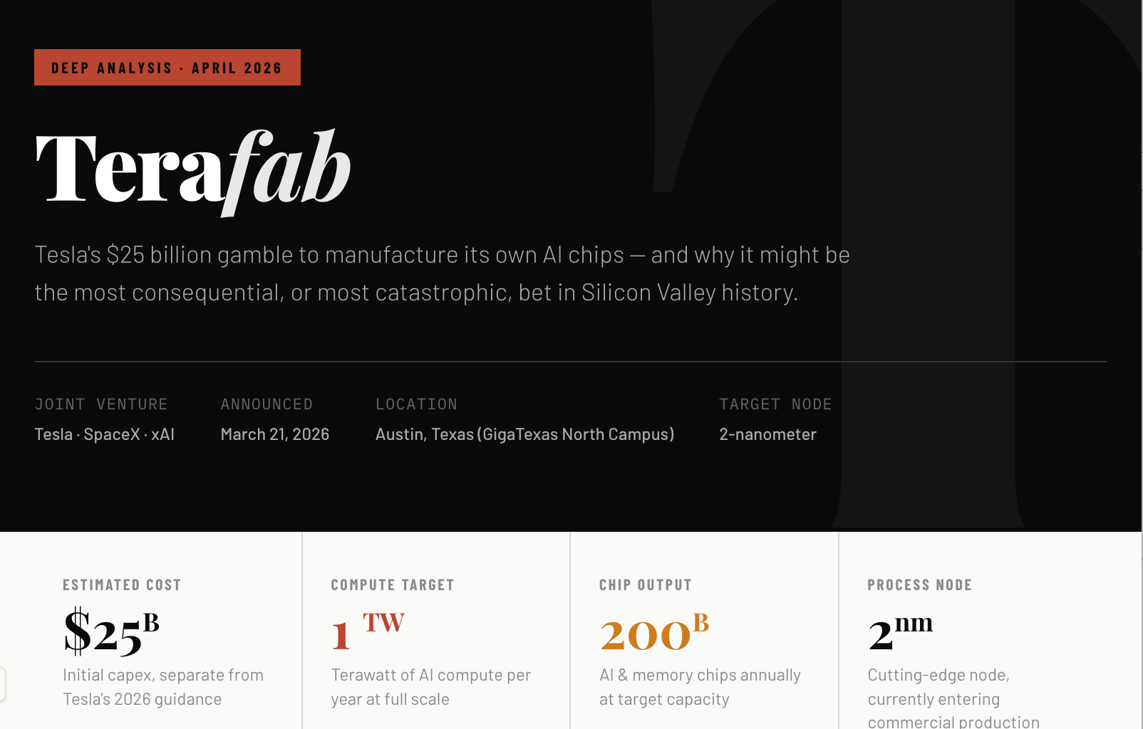

Tesla’s $25 billion gamble to manufacture its own AI chips — and why it might be the most consequential, or most catastrophic, bet in Silicon Valley history.
Joint Venture: Tesla · SpaceX · xAI | Announced: March 21, 2026 | Location: Austin, Texas (GigaTexas North Campus) | Target Node: 2-nanometer
| Metric | Figure |
|---|---|
| Estimated Cost | $25B (initial capex, separate from Tesla’s 2026 guidance) |
| Compute Target | 1 TW/year at full scale |
| Chip Output | 200B AI & memory chips annually at target capacity |
| Process Node | 2nm — cutting-edge, currently entering commercial production |
01 — Overview: What Terafab Actually Is
Terafab is a joint semiconductor fabrication venture between Tesla, SpaceX, and xAI — announced by Elon Musk on March 21, 2026 at Austin’s historic Seaholm Power Plant. It is the most ambitious attempt to build a vertically integrated chip factory from scratch in the modern era. The facility is planned for the North Campus of Giga Texas and is designed to consolidate every stage of semiconductor production under a single roof: chip design, lithography, fabrication, memory production, advanced packaging, and testing.
The stated rationale is straightforward: Tesla’s existing chip suppliers — primarily TSMC and Samsung — cannot expand production capacity at a rate compatible with Tesla’s projected demand for AI silicon powering its FSD systems, Cybercab robotaxis, and Optimus humanoid robots. Rather than waiting in queue, Musk is proposing to become his own foundry.
“We either build the Terafab, or we don’t have the chips, and we need the chips, so we build the Terafab.” — Elon Musk, Terafab Launch Event, March 21, 2026
The architectural ambition is genuinely novel. Existing chip fabs are highly specialized facilities that handle individual stages of production — wafers move between dozens of separate sites across continents. Terafab proposes to compress this entire supply chain into one location, enabling what Tesla calls a “make a chip, test it, revise the mask, and repeat” iteration loop that no other facility on Earth currently supports.
Terafab
Tesla’s $25 billion gamble to manufacture its own AI chips — and why it might be the most consequential, or most catastrophic, bet in Silicon Valley history.

AI Applications 1: Semiconductor Equipment Manufacturing, Engineering & Development
As an affiliate, we earn on qualifying purchases.
As an affiliate, we earn on qualifying purchases.
What Terafab Actually Is
Terafab is a joint semiconductor fabrication venture between Tesla, SpaceX, and xAI — announced by Elon Musk on March 21, 2026 at Austin’s historic Seaholm Power Plant. It is the most ambitious attempt to build a vertically integrated chip factory from scratch in the modern era. The facility is planned for the North Campus of Giga Texas and is designed to consolidate every stage of semiconductor production under a single roof: chip design, lithography, fabrication, memory production, advanced packaging, and testing.
The stated rationale is straightforward: Tesla’s existing chip suppliers — primarily TSMC and Samsung — cannot expand production capacity at a rate compatible with Tesla’s projected demand for AI silicon powering its FSD systems, Cybercab robotaxis, and Optimus humanoid robots. Rather than waiting in queue, Musk is proposing to become his own foundry.
“We either build the Terafab, or we don’t have the chips, and we need the chips, so we build the Terafab.”
— Elon Musk, Terafab Launch Event, March 21, 2026The architectural ambition is genuinely novel. Existing chip fabs are highly specialized facilities that handle individual stages of production — wafers move between dozens of separate sites across continents. Terafab proposes to compress this entire supply chain into one location, enabling what Tesla calls a “make a chip, test it, revise the mask, and repeat” iteration loop that no other facility on Earth currently supports.

Fundamentals of Semiconductor Fabrication
As an affiliate, we earn on qualifying purchases.
As an affiliate, we earn on qualifying purchases.
Why the Numbers Force This
The demand arithmetic behind Terafab is what makes the project feel less like ambition and more like necessity — at least in Musk’s framing. Tesla’s automotive business currently consumes a relatively modest number of chips compared to its ambitions in robotics and autonomous systems. That gap is about to become a chasm.
At GigaTexas alone — one facility — Tesla projects the capacity for 10 million Optimus robots per year. That requires roughly 20 million chips, which is approximately six times Tesla’s current chip demand across its entire automotive business. Scale to Tesla’s stated long-term target of 100 million Optimus robots annually, and the demand exceeds 200 billion chips — a number that would require Tesla to consume more than 50 times its current chip demand.
No single external supplier can commit to those volumes on Tesla’s timeline. TSMC is already at capacity for its 2nm process through the end of 2026. That supply ceiling is what transforms Terafab from an audacious optional project into, by Tesla’s own logic, an existential infrastructure play.
Total AI compute production per year globally — only ~2% of Tesla + SpaceX’s projected combined requirement
One terawatt of AI compute per year — 50× the current entire global annual AI compute production

Proceedings of the International Conference on Advanced Mechanical Engineering, Automation, and Sustainable Development 2021 (AMAS2021) (Lecture Notes in Mechanical Engineering)
As an affiliate, we earn on qualifying purchases.
As an affiliate, we earn on qualifying purchases.
The Chip Generation Ladder
Terafab is not a speculative project disconnected from existing products. Tesla has a clear generational chip roadmap, and Terafab is the infrastructure bet that enables the later generations to exist at meaningful scale.
The space computing angle is the most radical element of the Terafab vision. Musk argues that solar irradiance in low Earth orbit is roughly 5× greater than at Earth’s surface, and that heat rejection in vacuum makes thermal scaling viable in ways impossible on the ground. The full-scale Terafab is described as ultimately directing 80% of its compute output toward space-based orbital AI satellites — with only 20% for terrestrial applications.
AI chip testing and packaging equipment
As an affiliate, we earn on qualifying purchases.
As an affiliate, we earn on qualifying purchases.
The Vertical Integration Thesis
The core engineering proposition of Terafab — if it can be delivered — is genuinely disruptive to how the semiconductor industry currently works. Conventional chip production is a massively distributed, interdependent global supply chain. A single leading-edge chip requires lithography equipment from ASML in the Netherlands, photoresists from Japan, wafer polish from Korea, and advanced packaging facilities often in Southeast Asia. Wafers routinely cross international borders multiple times during production.
Terafab’s architectural claim is to collapse that chain into a single building — a “single-campus” iteration loop where the distance between mask revision and wafer test is measured in meters, not months. This is genuinely unprecedented at leading-edge process nodes. No existing fab — not TSMC’s most advanced Arizona facility, not Samsung’s Taylor plant — operates at this level of vertical integration.
“Make a chip, test it, revise the mask, and repeat without shipping wafers between sites — a capability that does not currently exist in any other chip fab globally.”
— Tesla, Terafab Technical Brief, March 2026The initial prototype facility at GigaTexas will target 100,000 wafer starts per month — matching the scale of a single TSMC advanced node facility. The long-term ambition scales to 1 million wafer starts per month, which would represent roughly 70% of TSMC’s entire current global output from a single site.
Beyond logic chips, Terafab plans to produce two distinct chip categories: inference processors optimized for Tesla’s ground-based AI applications (FSD, Optimus, Cybercab), and D3 space-hardened chips designed for orbital environments where radiation tolerance and vacuum thermal management are primary design constraints — chip types with essentially no commercial production precedent at scale.
Where Terafab Sits in the Landscape
| Entity | Type | 2nm Capability | Annual Output | Status |
|---|---|---|---|---|
| Terafab (Tesla/SpaceX/xAI) | IDM (Internal) | Planned | Target: 200B chips | Development |
| TSMC | Pure-play Foundry | Active (N2) | ~1.4M WSM global | Production |
| Samsung Foundry | IDM + Foundry | Slipping (2nm) | ~900K WSM global | Delayed |
| Intel Foundry | Foundry (spinoff) | 18A/14A roadmap | Ramping | Proving |
| Rapidus (Japan) | Gov-backed startup | 2nm target 2027 | Low volume initial | Pre-production |
| Nvidia (fabless) | Fabless (TSMC) | Via TSMC | High (TSMC-limited) | Production |
Tesla’s competitive position is unusual: it is attempting to enter a capital-intensive, expertise-dense industry that has historically only produced new players through government mandates or spinoffs from established IDMs. All recent new foundry entrants — Intel Foundry, Rapidus, Tata Semiconductor — have yet to prove competitive world-class manufacturing capability. The barriers are not just capital; they are accumulated institutional knowledge measured in decades.
The Numbers Behind the Numbers
Tesla’s financial position at the time of the Terafab announcement tells a complex story. The company ended 2025 with $44 billion in cash — substantial, but also the only cushion against a project whose true cost is contested even by Tesla’s own advisors.
Total cash reserves. The Terafab $25B estimate is not yet reflected in Tesla’s 2026 capex guidance, which already exceeds $20B separately.
Down 3% YoY. Automotive revenue fell 10% to $69.5B. Free cash flow was $6.2B on $8.5B capex — now set to more than double.
Tesla’s internal estimate. Morgan Stanley puts the true figure at $35–45B. Tom’s Hardware analysis suggests full-scale 1TW goal would cost $4–5 trillion over decades.
Earliest realistic chip output date under an aggressive build scenario. Volume at scale not before 2030, per most independent analysts.
The financial stretch is significant. Tesla is committing to more than double its capex level — on top of its existing $20B+ 2026 capex plan — while simultaneously navigating declining automotive revenue, a contested regulatory environment for FSD, and a share price that has been under pressure. Tesla’s own 10-K filing acknowledges the company may need to raise additional capital.
For full-scale ambitions — the 1 terawatt compute target — independent semiconductor analysis from Bernstein estimates Terafab would need 142 to 358 individual fab modules. At $15–20 billion per leading-edge fab module (the TSMC/Samsung benchmark), the capital requirement for full-scale realization runs into the trillions, not billions. This is a generational infrastructure bet, not a four-year project.
Bull Case vs. Bear Case
Battery Day Déjà Vu?
The most instructive comparison for Terafab is Tesla’s Battery Day presentation in September 2020, when Musk promised a revolution in battery manufacturing via the 4680 cell. Tesla was going to ramp to 10 GWh within a year and eventually reach 3 TWh by 2030 — enough to power 20 million vehicles annually. The dry electrode process was going to cut costs by 50%. Five and a half years later, the 4680 program remains a disappointment: the dry electrode process needed six or seven revisions, it took years longer than promised, and the 3 TWh target remains a distant vision.
The parallel is instructive but not dispositive. Tesla did eventually ship 4680 cells in production vehicles. The technology works — it just arrived late and at higher cost than promised. Terafab could follow the same trajectory: real, functional, but delayed and more expensive. The difference is that semiconductor manufacturing at 2nm is arguably more technically demanding than battery cell production, and the precision required at leading-edge nodes leaves considerably less margin for the iterative improvisation that has historically characterized Tesla’s manufacturing approach.
What Musk is proposing is also genuinely unprecedented in scale and integration ambition — not quite comparable to anything attempted in the commercial semiconductor industry. The closest historical analogy might be IBM’s early vertical integration in mainframe computing: an era when one company could own the full stack from silicon to software to systems. That era ended precisely because the complexity required specialization. Terafab is, in a sense, a bet that AI-age computing requirements are so extreme that vertical integration becomes viable again — perhaps even necessary.
The Most Consequential Chip Bet of the Decade
Terafab is simultaneously the most rational response to a genuine supply constraint and the most technically audacious semiconductor project ever attempted by a company with no fab experience. The demand math is real: if Optimus scales anywhere near Musk’s projections, the chip volumes required are simply incompatible with external supply at any price. The project is not irrational — it is, in the Musk tradition, a bet that execution can overcome institutional complexity.
The execution risk, however, is profound. The semiconductor industry’s barriers to entry are not primarily financial — they are accumulated process knowledge, specialized equipment relationships (particularly with ASML for EUV lithography), and a global talent pool that is already oversubscribed by TSMC, Samsung, and Intel. Morgan Stanley’s estimate that the first Terafab chips will not arrive until 2028 is optimistic by industry-watchers’ standards.
The most realistic near-term outcome is a functional prototype facility at GigaTexas that validates the iteration-loop thesis and produces AI5 chips in small volumes, while the full-scale 1-terawatt vision remains a multi-decade, multi-company infrastructure program. That alone — a working advanced fab producing Tesla’s own silicon — would still constitute one of the most significant industrial achievements of the 2020s. Whether it arrives on Musk’s timeline, on anyone’s timeline, or at all, is the trillion-dollar question.
02 — Demand Driver: Why the Numbers Force This
The demand arithmetic behind Terafab is what makes the project feel less like ambition and more like necessity — at least in Musk’s framing. Tesla’s automotive business currently consumes a relatively modest number of chips compared to its ambitions in robotics and autonomous systems. That gap is about to become a chasm.
Annual chip demand — Tesla’s scaling trajectory:
| Scenario | Estimated Annual Chip Demand |
|---|---|
| Current automotive (AI4) | ~35 million |
| Cybercab + FSD at scale | ~80 million |
| 10M Optimus robots/year | ~20 billion |
| 100M Optimus robots/year | 200 billion+ |
Source: Morgan Stanley estimates, Tesla projections. GigaTexas alone = capacity for 10M Optimus/yr = 20M chips = ~6× Tesla’s entire current chip demand across all automotive.
At GigaTexas alone — one facility — Tesla projects capacity for 10 million Optimus robots per year. That requires roughly 20 million chips, approximately six times Tesla’s current chip demand across its entire automotive business. Scale to Tesla’s stated long-term target of 100 million Optimus robots annually, and demand exceeds 200 billion chips — more than 50 times current demand.
No single external supplier can commit to those volumes on Tesla’s timeline. TSMC is already at capacity for its 2nm process through the end of 2026. That supply ceiling is what transforms Terafab from an audacious optional project into, by Tesla’s own logic, an existential infrastructure play.
Key scale figures:
- ~20 GW/year — total global AI compute production today, roughly 2% of Tesla + SpaceX’s projected combined requirement
- 1 TW/year — Terafab’s ultimate target, 50× the current entire global annual AI compute output
03 — Silicon Roadmap: The Chip Generation Ladder
Terafab is not a speculative project disconnected from existing products. Tesla has a clear generational chip roadmap, and Terafab is the infrastructure bet that enables the later generations to exist at meaningful scale.
AI4 — Current Production Chip (Now · Samsung-manufactured)
Powers mainstream Tesla vehicles, Full Self-Driving, and the Cybercab Robotaxi. The baseline against which all successor generations are measured.
AI5 — First Terafab Product (Small batch 2026 · Volume 2027)
40–50× more compute and 9× more memory than AI4. The core chip for Optimus humanoid robots and next-generation FSD. Among the first products the Terafab pilot facility is designed to produce. Initially TSMC-manufactured; migrating in-house.
AI6 — Optimus Scale Chip (2027–2028 · Samsung $16.5B agreement)
Part of a $16.5 billion Samsung production agreement. Targeted primarily at Optimus robot scaling. AI6 has already experienced roughly six months of delay due to Samsung’s 2nm production slipping.
AI7 / AI8 — Orbital AI Infrastructure (2029+ · Space-optimized)
Theorized for space-based orbital data centers operated by xAI and SpaceX. Terafab’s D3 chip category — hardened for vacuum and radiation environments — is the enabling platform. Musk argues solar irradiance in LEO is ~5× greater than at Earth’s surface, and heat rejection in vacuum makes thermal scaling viable in ways impossible on the ground.
The full-scale Terafab is described as ultimately directing 80% of its compute output toward space-based orbital AI satellites, with only 20% for terrestrial applications.
04 — Technical Architecture: The Vertical Integration Thesis
The core engineering proposition of Terafab — if it can be delivered — is genuinely disruptive to how the semiconductor industry currently works. Conventional chip production is a massively distributed, interdependent global supply chain. A single leading-edge chip requires lithography equipment from ASML in the Netherlands, photoresists from Japan, wafer polish from Korea, and advanced packaging often in Southeast Asia. Wafers routinely cross international borders multiple times during production.
Terafab’s architectural claim is to collapse that chain into a single building — a “single-campus” iteration loop where the distance between mask revision and wafer test is measured in meters, not months. This is genuinely unprecedented at leading-edge process nodes. No existing fab — not TSMC’s most advanced Arizona facility, not Samsung’s Taylor plant — operates at this level of vertical integration.
“Make a chip, test it, revise the mask, and repeat without shipping wafers between sites — a capability that does not currently exist in any other chip fab globally.” — Tesla, Terafab Technical Brief, March 2026
The initial prototype facility at GigaTexas targets 100,000 wafer starts per month — matching the scale of a single TSMC advanced node facility. The long-term ambition scales to 1 million wafer starts per month, which would represent roughly 70% of TSMC’s entire current global output from a single site.
Beyond logic chips, Terafab plans to produce two distinct chip categories:
- Inference processors — optimized for Tesla’s ground-based AI applications (FSD, Optimus, Cybercab)
- D3 space-hardened chips — designed for orbital environments where radiation tolerance and vacuum thermal management are primary design constraints, with essentially no commercial production precedent at scale
05 — Competitive Context: Where Terafab Sits in the Landscape
| Entity | Type | 2nm Capability | Annual Output | Status |
|---|---|---|---|---|
| Terafab (Tesla/SpaceX/xAI) | IDM (Internal) | Planned | Target: 200B chips | Development |
| TSMC | Pure-play Foundry | Active (N2) | ~1.4M WSM global | Production |
| Samsung Foundry | IDM + Foundry | Slipping (2nm) | ~900K WSM global | Delayed |
| Intel Foundry | Foundry (spinoff) | 18A/14A roadmap | Ramping | Proving |
| Rapidus (Japan) | Gov-backed startup | 2nm target 2027 | Low volume initial | Pre-production |
| Nvidia (fabless) | Fabless (TSMC) | Via TSMC | High (TSMC-limited) | Production |
Tesla’s competitive position is unusual: it is attempting to enter a capital-intensive, expertise-dense industry that has historically only produced new players through government mandates or spinoffs from established IDMs. All recent new foundry entrants — Intel Foundry, Rapidus, Tata Semiconductor — have yet to prove competitive world-class manufacturing capability. The barriers are not just capital; they are accumulated institutional knowledge measured in decades.
06 — Financial Reality: The Numbers Behind the Numbers
Tesla’s financial position at the time of the Terafab announcement tells a complex story. The company ended 2025 with $44 billion in cash — substantial, but also the only cushion against a project whose true cost is contested even by Tesla’s own advisors.
| Metric | Figure | Context |
|---|---|---|
| Tesla cash (end 2025) | $44B | Terafab costs not yet in 2026 capex guidance |
| 2025 revenue | $94.8B (−3% YoY) | Automotive revenue fell 10% to $69.5B |
| 2025 free cash flow | $6.2B on $8.5B capex | Capex now set to more than double |
| Terafab cost (Tesla est.) | $20–25B | Morgan Stanley: $35–45B; full 1TW scale: $4–5T |
| First chip output (MS est.) | 2028+ earliest | Volume at scale not before 2030 per most analysts |
The financial stretch is significant. Tesla is committing to more than double its capex level — on top of its existing $20B+ 2026 plan — while navigating declining automotive revenue, a contested FSD regulatory environment, and a share price under pressure. Tesla’s own 10-K filing acknowledges the company may need to raise additional capital.
For full-scale ambitions — the 1 terawatt compute target — Bernstein estimates Terafab would need 142 to 358 individual fab modules. At $15–20 billion per leading-edge fab module, the capital requirement for full-scale realization runs into the trillions. This is a generational infrastructure bet, not a four-year project.
07 — Investment Thesis: Bull Case vs. Bear Case
▲ Bull Case
- Tesla owns the full stack — chip to vehicle to robot. No supplier can hold it hostage on pricing, allocation, or roadmap timing.
- Optimus demand projections make external supply structurally impossible. A proprietary fab is the only path to 100M+ robots annually.
- Vertical integration at 2nm positions Tesla as one of a handful of entities producing cutting-edge AI silicon — a potential licensing or supply business beyond its own needs.
- Space computing is an unaddressed market. D3 space-hardened chips at scale have no current commercial competition.
- SpaceX’s potential IPO could provide additional capital runway and structural separation of fab risk from Tesla’s balance sheet.
▼ Bear Case
- Semiconductor manufacturing is a decades-long expertise accumulation. Tesla has zero fab process history. TSMC took 30+ years to reach its current position.
- True cost is likely 2–10× the stated $25B estimate. Full 1TW vision requires capital in the trillions — impossible on Tesla’s current balance sheet.
- Qualified fab construction workers and process engineers are genuinely scarce. TSMC’s Arizona Fab 21 Phase 1 was repeatedly delayed for exactly this reason.
- Tesla’s track record with ambitious manufacturing timelines is poor — 4680 battery cells took 5+ years beyond initial targets and still underperform projections.
- Revenue declined in 2025. Doubling capex while cash flow tightens and automotive margin compresses creates real balance sheet risk.
08 — Historical Parallel: Battery Day Déjà Vu?
The most instructive comparison for Terafab is Tesla’s Battery Day presentation in September 2020, when Musk promised a revolution in battery manufacturing via the 4680 cell. Tesla was going to ramp to 10 GWh within a year and eventually reach 3 TWh by 2030. The dry electrode process was going to cut costs by 50%. Five and a half years later, the 4680 program remains a disappointment: the dry electrode process needed six or seven revisions, it took years longer than promised, and the 3 TWh target remains a distant vision.
The parallel is instructive but not dispositive. Tesla did eventually ship 4680 cells in production vehicles. The technology works — it just arrived late and at higher cost than promised. Terafab could follow the same trajectory: real, functional, but delayed and more expensive. The difference is that semiconductor manufacturing at 2nm is arguably more technically demanding than battery cell production, and the precision required at leading-edge nodes leaves considerably less margin for the iterative improvisation that has historically characterized Tesla’s manufacturing approach.
What Musk is proposing is also genuinely unprecedented in scale and integration ambition. The closest historical analogy might be IBM’s early vertical integration in mainframe computing — an era when one company could own the full stack from silicon to software to systems. That era ended precisely because the complexity required specialization. Terafab is, in a sense, a bet that AI-age computing requirements are so extreme that vertical integration becomes viable again — perhaps even necessary.
Editorial Verdict
Terafab is simultaneously the most rational response to a genuine supply constraint and the most technically audacious semiconductor project ever attempted by a company with no fab experience.
The demand math is real: if Optimus scales anywhere near Musk’s projections, the chip volumes required are simply incompatible with external supply at any price. The project is not irrational — it is, in the Musk tradition, a bet that execution can overcome institutional complexity.
The execution risk, however, is profound. The semiconductor industry’s barriers to entry are not primarily financial — they are accumulated process knowledge, specialized equipment relationships (particularly with ASML for EUV lithography), and a global talent pool already oversubscribed by TSMC, Samsung, and Intel. Morgan Stanley’s estimate that the first Terafab chips will not arrive until 2028 is optimistic by industry-watchers’ standards.
The most realistic near-term outcome is a functional prototype facility at GigaTexas that validates the iteration-loop thesis and produces AI5 chips in small volumes, while the full-scale 1-terawatt vision remains a multi-decade, multi-company infrastructure program. That alone — a working advanced fab producing Tesla’s own silicon — would still constitute one of the most significant industrial achievements of the 2020s. Whether it arrives on Musk’s timeline, on anyone’s timeline, or at all, is the trillion-dollar question.
Analysis based on public disclosures, analyst reports (Morgan Stanley, Bernstein), and industry sources as of April 2026. Chip demand projections derived from Tesla/SpaceX event materials and Morgan Stanley research. Cost estimates reflect range across Tesla internal guidance ($20–25B), Morgan Stanley ($35–45B), and Tom’s Hardware/Bernstein full-scale modelling ($4–5T). This analysis does not constitute investment advice.