
This breakthrough photonic chip can dramatically boost AI performance by offering ultra-fast data processing speeds, reaching over 5.3 Tbps/mm² with just 120 femtojoules per bit. It performs neural network tasks optically, reducing energy use by 10 to 100 times and cutting latency drastically. Its scalable manufacturing and compatibility with electronic systems mean wide adoption is possible. To discover how this innovation could reshape AI technology, explore the details further.
Key Takeaways
- Achieves ultra-high bandwidth density of 5.3 Tbps/mm² and 800 Gbps total throughput, enabling faster AI processing.
- Uses optical neural networks to perform complex AI tasks with over 92% accuracy at speeds under half a nanosecond.
- Significantly reduces energy consumption, consuming just 120 femtojoules per bit, lowering operational costs.
- Integrates scalable photonic and electronic components on silicon, supporting compact, high-performance AI hardware.
- Facilitates real-time AI applications across models like ResNet and BERT, transforming AI speed and efficiency.

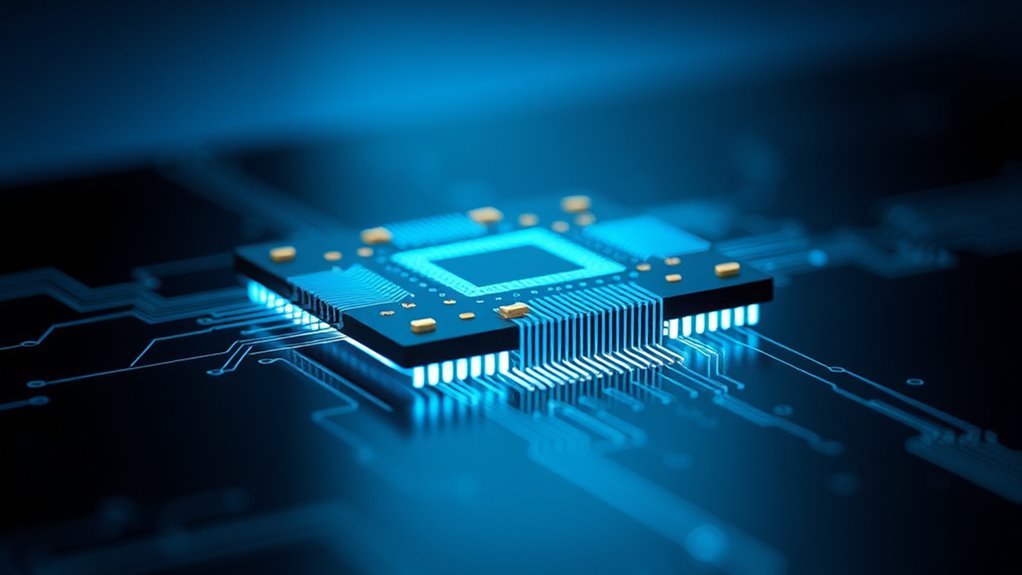
Photonic chips are revolutionizing AI technology by offering faster, more energy-efficient data processing. Imagine handling massive AI workloads with considerably reduced power consumption and almost instantaneous speeds. Columbia Engineering has developed a groundbreaking 3D-integrated photonic-electronic chip that achieves a bandwidth density of 5.3 terabits per second per square millimeter and a total bandwidth of 800 gigabits per second. Remarkably, it consumes only 120 femtojoules per bit, making data transfer energy costs nearly negligible compared to traditional electronic chips. This reduction in power consumption—by a factor of 10 to 100 times—means your AI systems can operate faster without the usual heat and energy constraints, enabling more compact and energy-efficient hardware. This innovation is based on a decade of research in optical neural networks and photonic computing. The integration techniques underpinning this technology are equally impressive. You can think of these chips as combining photonic devices with CMOS electronics using scalable manufacturing processes from commercial foundries. The vertical 3D stacking of six photonic chips supports an astonishing 50 billion transistors and a million photonic components within a compact package. Proprietary Thin-Film Lithium Niobate on Insulator (TFLNoI) technology allows precise, high-quality photonic circuits directly on silicon wafers, ensuring compatibility with existing electronic systems. This integration not only boosts speed but also simplifies the process of embedding photonic elements on-chip, eliminating reliance on slower, off-chip electronics. The scalability of manufacturing processes is crucial for bringing this technology from research labs to widespread commercial use, making advanced photonic AI processors more accessible. When it comes to computational power, these photonic processors excel at executing complex AI models such as ResNet, BERT, and deep reinforcement learning. They perform key neural network calculations optically, achieving over 92% classification accuracy—comparable to traditional digital systems—without needing special training modifications. They accelerate core AI tasks like convolution operations, matrix multiplications, and non-linear functions, all while consuming near-zero energy. This capability extends to handling large data volumes rapidly, thanks to high bandwidth density and minimized electronic bottlenecks, which drastically cut down processing times. Speed and latency are where these chips truly shine. Optical neural networks can perform critical computations in less than half a nanosecond, enabling real-time AI processing. By leveraging multiple wavelengths of light, they process several data streams simultaneously, increasing throughput exponentially. Overall, the use of light instead of electrons reduces latency and unblocks new levels of performance, making these photonic chips a transformative leap forward for AI technology.
Top picks for "breakthrough photonic chip"
Open Amazon search results for this keyword.
As an affiliate, we earn on qualifying purchases.
Frequently Asked Questions
How Does the Photonic Chip Compare to Traditional Electronic Chips?
You’ll find photonic chips vastly outperform traditional electronic chips in speed, efficiency, and power use. They deliver up to 18 times higher computational throughput, run at a fraction of the power, and generate far less heat. This means faster training, lower latency, and more sustainable AI operations. With higher memory bandwidth and scalable fabrication, photonic chips enable more advanced AI tasks while reducing cooling costs and energy consumption markedly.
What Are the Main Challenges in Commercializing Photonic AI Chips?
You face several main challenges in commercializing photonic AI chips. First, achieving high channel counts and scalability requires advances in materials and fabrication techniques. You also need to manage manufacturing complexities, like maintaining surface quality and precise packaging. Additionally, integrating these chips into existing ecosystems demands collaboration across industries. Overcoming high costs, ensuring reliability, and reducing power consumption are vital for widespread adoption and realizing photonics’ full potential.
Can Photonic Chips Be Integrated With Existing AI Hardware?
You can definitely integrate photonic chips with existing AI hardware, and it’s like hitting two birds with one stone. These chips work seamlessly with CMOS electronics, thanks to hybrid platforms and advanced bonding techniques. You’ll find they complement current systems by boosting bandwidth and reducing power consumption. With proper mapping of neural networks and addressing memory needs, integrating photonics into your AI infrastructure becomes not just feasible but a game-changer.
What Industries Will Benefit Most From This Technology?
You’ll see the biggest benefits in telecommunications, data centers, scientific research, and energy sectors. Photonic chips boost data transfer speeds, reduce latency, and cut energy use, making these industries more efficient and sustainable. In telecom, they support high-bandwidth networks. Scientific fields like physics and astronomy run faster simulations, while energy sectors see lower power demands. Overall, these chips help industries achieve higher performance with less environmental impact.
How Scalable Is the Production of These Photonic Chips?
You’ll find that producing these photonic chips is challenging but becoming more scalable. Advances in automation, wafer-level packaging, and expanding foundry capabilities are key to increasing production speed and volume. While current manufacturing involves complex, costly steps, ongoing innovations aim to simplify and automate processes. With more open-access foundries and improved integration techniques, mass production could reach millions of units weekly, making widespread deployment more feasible in the near future.
Conclusion
This breakthrough photonic chip could completely transform AI as you know it. Imagine faster, more efficient processing that unearths capabilities we haven’t even dreamed of yet. But the real question is—what’s coming next? Will this innovation truly unleash a new era of technology, or will unforeseen challenges slow its progress? Stay tuned, because the future of AI might be closer than you think, and it’s more exciting than ever.