
By Thorsten Meyer
Every few weeks a headline announces that China has cracked the last hard problem in chipmaking. A secret EUV prototype in Shenzhen. A homegrown lithography machine entering mass production. A domestic tool hitting a 90 percent yield. Each one triggers the same reflex — a spike of alarm in Western policy circles, a mirror-image spike of triumphalism in Chinese media, and a market lurch in whichever direction the mood is running that day.
And each one is, almost without exception, an overreaction — in both directions. The alarmists read a prototype as a fait accompli. The triumphalists read a shipped machine as a solved problem. Both are making the same mistake: treating semiconductor manufacturing as a knowledge problem, where the answer, once discovered, can be copied. It is not. It is a learning-by-doing problem, where the answer has to be earned through years of running the actual process at scale — and that kind of knowledge cannot be stolen, bought, or teleported. It has to be lived through.
This is the wall China is climbing. It is real, it is being climbed, and it is much taller than either the alarm or the triumph admits. Let me lay out where things actually stand, because the honest picture is more interesting than either caricature.
Every few weeks a headline says China cracked the last hard problem in chipmaking — and triggers alarm in one camp, triumph in the other. Both overreact, because both mistake a learning-by-doing problem for a copying problem. It isn’t one.
▲ Forward-looking · figures are point-in-time estimates“A machine exists” and “a machine makes advanced chips at scale, profitably, for years” are separated by a chasm — made of things that only accumulate with time.
In a race, a burst of speed closes the gap. In a phase transition, you can’t move faster to cross over — you have to accumulate enough, slowly, until the system changes state.
When you see “China achieves X,” ask which of two very different claims is actually being made.
Even amid the loud headlines, the quiet data points all say the same thing.
No prototype, no shipped tool, no yield headline teleports past it.
What is genuinely happening
Start with the real progress, because it is real and dismissing it is its own kind of error.
China has, by multiple credible accounts, begun mass-producing domestic immersion DUV lithography machines — the most advanced class of tool available to it after export controls cut off EUV. The systems, tied to Huawei-linked firms and evaluated at SMIC, target 28-nanometer manufacturing with single exposure and, through multi-patterning, are believed capable of reaching 7-nanometer and potentially 5-nanometer nodes. Most components are domestically sourced. And separately, Reuters reported a domestic EUV machine at the prototype stage. This is not nothing. A country that a decade ago could not build these tools at all is now shipping early units of the second-most-advanced class and prototyping the most advanced.
At the same time, SMIC has demonstrated 7-nanometer production using older DUV immersion tools through multi-patterning — the Huawei chips everyone has seen — and is reportedly developing 5-nanometer capability. Huawei's stated ambition runs to over a million high-end AI-accelerator dies this year. The direction of travel is unambiguous: China is moving up the stack, deliberately and with enormous state backing, and it will keep moving.
So the triumphalist headline is not fabricated. It is just radically incomplete.
As an affiliate, we earn on qualifying purchases.
What the headline leaves out: the four walls behind the wall
Here is what the announcements skip, and it is the whole substance of the matter. "A machine exists" and "a machine produces advanced chips at scale, profitably, reliably, for years" are separated by a chasm, and the chasm is made of things that only accumulate with time.
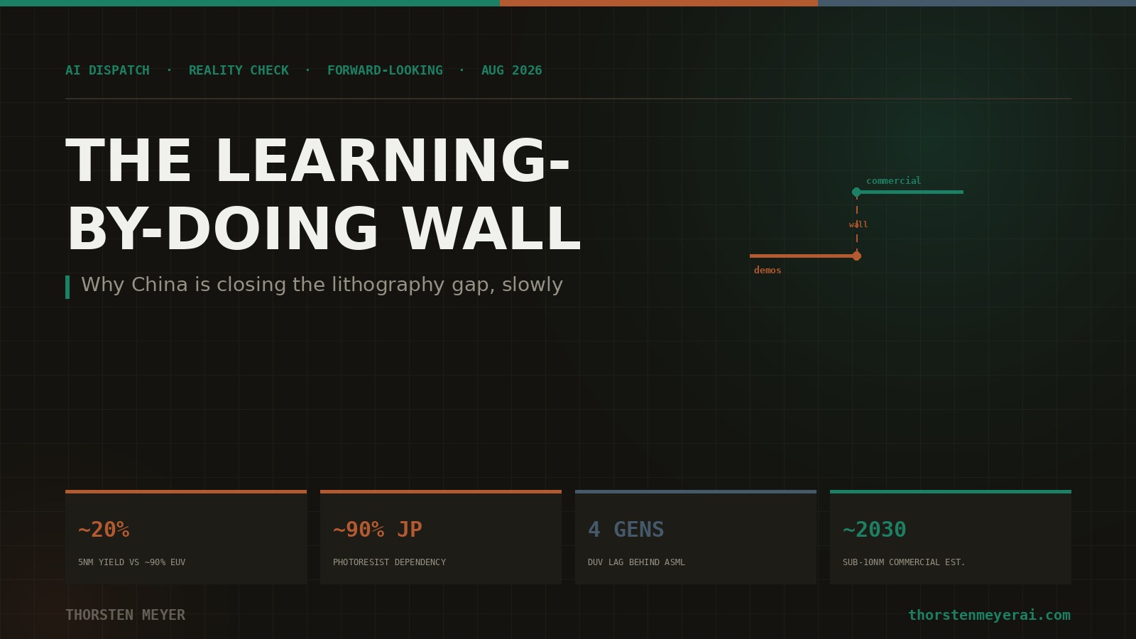
Yield. SMIC can make 5-nanometer chips; it reportedly makes them at yields around 20 percent, against the roughly 90 percent a leading fab achieves with EUV. Yield is the difference between a demonstration and a business. A process that throws away four of every five dies is not a manufacturing capability, it is a science experiment that occasionally works — and closing that gap is not a matter of one clever fix but of ten thousand small ones, each learned by running wafers and studying what went wrong.
Materials. Even a perfect machine needs ultra-pure inputs, and here China is deeply dependent on exactly the suppliers it is trying to route around. It buys roughly 90 percent of its high-end photoresist — the light-sensitive chemical that is the photographic film of chipmaking — from Japan, because Japanese firms have a purity capability that took decades to build and that China cannot yet match. You can build the camera and still be unable to make the film.
The generational lag. By sober assessments, China's domestic DUV tools lag ASML by something like four generations — roughly equivalent to the Dutch company's tools of fifteen years ago. ASML's own leadership has put China ten to fifteen years behind. And credible independent forecasts do not expect domestically-made tools to reach sub-10-nanometer commercial production before around 2030. Not a prototype that makes a few chips under controlled conditions — commercial production, the thing that actually matters.
The servicing dependency. The two hundred-plus advanced DUV tools already installed in China are not self-maintaining. Multi-patterning at high utilization is brutal on optics, which drift out of calibration and need constant expert servicing — servicing that still depends on ASML and its partners. The installed base is a borrowed capability, not an owned one, for as long as the maintenance chain runs through the West.
high-end photoresist for chip manufacturing
As an affiliate, we earn on qualifying purchases.
As an affiliate, we earn on qualifying purchases.
Why this is a phase transition, not a race
The framing I keep coming back to is that this is a phase transition, not a footrace, and the distinction is the whole point.
In a footrace, the gap is measured in distance, and a burst of speed closes it. In a phase transition, you cannot get from one state to the next by moving faster — you have to accumulate enough of something, slowly, until the system crosses over. Water does not become steam by heating faster; it becomes steam when enough heat has gone in, at the temperature physics dictates, and not one degree before. Advanced chip manufacturing is like that. The capability does not arrive when you have the blueprint or even the machine. It arrives when you have run the process long enough, at enough scale, fixing enough failures, that the tacit knowledge of how to actually do it has accumulated in the engineers, the suppliers, the equipment, and the institutional memory of the fab.
That accumulated, hard-won, mostly-undocumented knowledge is what economists call learning-by-doing, and its defining property is that it cannot be transferred. ASML did not become ASML by reading a manual; it became ASML through decades of intimate collaboration with TSMC, Samsung, and Intel, each generation of tool co-developed with the leading fabs pushing the frontier, each failure teaching something no document captured. China is trying to build that same knowledge largely in isolation, with chipmakers who have mostly been playing catch-up rather than pushing the edge — which means it must not only climb the wall but do so without the climbing partners that made the ascent possible for everyone before it.
This is why the timelines are measured in years and not quarters, and why they resist acceleration by money. You can buy machines. You cannot buy the fifteen years of operating experience that makes the machines produce yield. The state can pour capital in — and it is — but capital shortens some steps and not others, and the learning steps are the ones it shortens least.
ultraviolet EUV lithography equipment
As an affiliate, we earn on qualifying purchases.
As an affiliate, we earn on qualifying purchases.
What this means for how to read the news
So here is the discipline I apply to every one of these headlines, and I would recommend it to anyone trying to invest, build, or set policy around this.
When you see "China achieves X," ask which of two very different claims is actually being made. Is it a machine functioned — a prototype produced light, a tool made a few chips, a demonstration succeeded? Or is it large-scale commercial production began — sustained yield, reliable uptime, years of operation, an actual business? The gap between those two is where almost all the real difficulty lives, and almost all the coverage collapses them into one. The alarmist reads the first as if it were the second. The triumphalist does the same. Both are wrong for the same reason.
And notice how the sober signals confirm the slow read even amid the loud ones. Chinese media itself went quiet on domestic-tool progress and even moved to deny an inflated yield claim — a tell that the insiders know the gap between demonstration and production better than the headlines do. ASML's China sales are falling as a share of its business but China still cannot do without its tools. The domestic machine ships in units of five this year, twenty next year — real, and a rounding error against what a single leading fab installs. Every sober data point says the same thing: genuine progress, stubbornly slow, on a timeline that no announcement compresses.
cleanroom equipment for semiconductor fabrication
As an affiliate, we earn on qualifying purchases.
As an affiliate, we earn on qualifying purchases.
The dispatch in one line
China is closing the lithography gap. It is doing so genuinely, with real machines and real state resolve, and it will keep closing it. But the gap is a learning-by-doing wall, not a footrace — a phase transition that requires accumulating tacit, unbuyable, untransferable operating knowledge over years, and no prototype, no shipped tool, and no yield headline teleports past it. The market overreacts to each announcement in whichever direction the mood favors, because it keeps mistaking a knowledge problem for a copying problem. It is not. The wall is real, it is being climbed, and it is taller than either the fear or the triumph will admit. Read every headline through that lens and you will be wrong far less often than the people reacting to them.
Analysis and opinion from a builder, founder, and post-labor economist running a local-first inference operation; a companion to the AI-hardware essay. Sources: The Diplomat and AI Futures Project on China's EUV/DUV progress and the photoresist dependency; Asia Times, TrendForce, Tech Startups, and The Information on the domestic immersion-DUV mass-production reports and the four-generation lag; AEI's "Lithography Loophole" report and follow-on analysis on SMIC/Huawei DUV multi-patterning, ~20% 5nm yields, and the servicing dependency; ASML commentary on the 10–15-year estimate; independent forecasts on the ~2030 sub-10nm commercial timeline. Figures are point-in-time estimates, several single-source, and forecasts are inherently uncertain. Not investment advice. Point-in-time as of 11 August 2026.